Field Emission SEM
The scanning electron microscope (SEM) uses a focused beam of high-energy electrons
to generate a variety of signals at the surface of solid specimens. The signals that
derive from electron-sample interactions produce information about the sample, including
surface structure (topology), chemical composition and crystalline structure and orientation.
Secondary electrons (SE) and backscattered electrons (BSE) are commonly used for imaging
samples: SEs are most valuable for showing morphology and topography on samples and
BSEs are most valuable for illustrating contrasts in composition in multiphase samples
(i.e. for rapid phase discrimination). X-ray generated by inelastic interaction is
used to determine chemical composition of the sample by energy dispersive X-ray spectroscopy
(EDS) technique. Crystal orientation of the grains in the sample can be analyzed by
electron backscatter diffraction (EBSD) technique. Nanometer-scale fabrication can
be performed by e-beam lithography, Nabity Nanometer Pattern Generating System (NPGS).
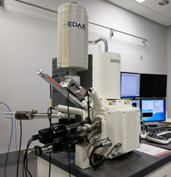
- Field Emission SEM, Supra 55 VP from Zeiss
- This Analytical Ultra High Resolution FESEM (~ 4nm) has variable pressure option to characterize beam sensitive and non-conducting samples.
- SUPRA 55 FESEM is equipped with the following detectors.
- SE, BSE, and CL detectors
- STEM detector
- In-lens detector
- EDS detector (EDAX Genesis) for chemical analysis in point, line or map scan modes
- EBSD detector (TSL-EDAX Digiscan) for crystal orientation imaging and mapping
- E-beam lithography (Nabity NPGS)
Instrument Manager: Ola Habboub
Backup: Dae-Young Jung