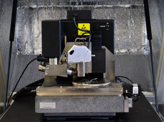
Atomic Force Microscope (AFM) is used for 3D imaging of conducting and non-conducting sample surfaces. It is a valuable tool for failure analysis and is indispensable for FAB process control. ADL has a multi-mode scanning probe system, Dimension 3100 microscope with Nanoscope V controller from Bruker (previously Veeco Instruments). It can achieve sub nm vertical resolution and nm lateral resolution. Maximum Scan area is 100 μm x 100 μm with max vertical range of ~ 8 μm. It is equipped with accessories that enable the following scanning modes:
- Atomic Force Microscopy (AFM) in the tapping and contact modes to measure surface topography, roughness, film thickness, feature size etc.
- Phase imaging AFM for variations in composition, adhesion, friction, viscoelasticity, differentiating regions of high and low surface adhesion/hardness; contaminant identification, mapping of components in composite materials.
- Conductive AFM for mapping of electrical conductivity across medium- to low-conducting and semiconducting materials.
- Scanning Tunneling Microscopy (STM) for topography of surface electronic states.
- Magnetic Force Microscopy (MFM) for domain structures in magnetic materials.
- Nano-manipulation/Nano-lithography for manipulation of nanoscale objects; anodic oxidation for fabrication of nano-patterns at localized areas.
- Scanning Capacitance Microscopy (SCM) to map variations in electron (hole) concentration on the surface of a doped semiconductor.
- Nano-indentation to measure mechanical properties by nano-indentations, nano-scratching and wear testing for film adhesion and durability studies.
- Force Modulation Microscopy to determine relative elasticity/stiffness of surface features.
- Fluid cell measurement for AFM imaging of samples in a liquid environment.
Instrument Manager: Anju Sharma