Lasers turn ordinary parchment paper into high-performance electronic circuits
Researchers create a platform for biodegradable, fully integrated circuits — no silicon, no toxic metals, no clean room required

What if the next generation of disposable electronics — the sensors in your food packaging, the diagnostic strips in a medical clinic, the environmental monitors scattered across a farm — were built not on silicon or plastic, but on a sheet of paper you could buy at the grocery store?
That vision just moved significantly closer to reality. A research team at Binghamton University’s Bioelectronics and Microsystems Laboratory, led by Professor Seokheun “Sean” Choi, has developed a new fabrication technique that uses a standard carbon dioxide laser to write electronic circuits directly onto commercial parchment paper — the same silicone-coated baking paper found in kitchens worldwide.
The work has been accepted for publication in ACS Applied Materials & Interfaces, one of the leading journals in the field of materials science.
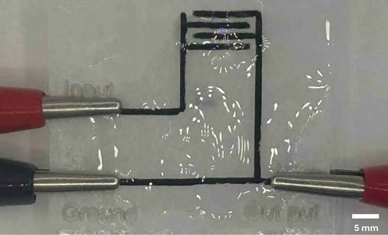
The technique is deceptively simple. Parchment paper is naturally water-repellent thanks to a thin silicone coating on its surface. By precisely targeting the paper with a laser, the team selectively removes that coating in specific patterns, exposing the water-absorbing cellulose fibers underneath. These laser-written channels then act as microscopic highways that guide water-based conductive inks exactly where they need to go — forming resistors, capacitors, interconnects, and even complete analog filter circuits, all on a single sheet of paper.
“The laser essentially writes wettability onto an unwettable surface,” said Choi, a professor in the Department of Electrical and Computer Engineering at the Thomas J. Watson College of Engineering and Applied Science. “Wherever the laser touches, the paper becomes receptive to our functional inks. Everywhere else, the silicone coating acts as a natural insulator.”
A decade-long quest
The new work represents the culmination of more than a decade of research in Choi’s lab on what he calls “papertronics” — the emerging field of paper-based electronics. Choi has been one of the pioneering researchers in this space since arriving at Binghamton, driven by a central question: Can paper replace silicon and plastic for disposable, single-use electronic devices?
The journey began with biobatteries. In 2015, Choi’s team built their first paper-based battery — a foldable device that looked like a matchbook and generated electricity from bacteria. That early prototype sparked a series of innovations: a ninja-star-shaped origami battery, saliva-activated biobatteries for emergency diagnostics, sweat-powered wearable energy harvesters, and even an ingestible capsule biobattery designed to operate inside the human gut.
Along the way, the lab also developed paper-based biosensors for point-of-care diagnostics, antimicrobial susceptibility testing, and environmental monitoring — all powered by the bacteria that naturally inhabit our world.
“My long-term vision has always been to create a complete, self-powered, disposable electronic system on paper,” Choi said. “We started with the power source — the biobattery. Then we moved to sensors. The missing piece was the circuit itself: the resistors, capacitors, and interconnects that tie everything together.”
That missing piece arrived in 2024, when Choi’s team demonstrated the first fully integrated paper circuit board — complete with tunable resistors, capacitors, and transistors — on a single sheet of chromatography paper using wax-printed patterns to guide ink deposition. The work, published in Advanced Sustainable Systems, proved the concept but revealed a stubborn limitation: the wax barriers used to define circuit features blurred and spread when heated, limiting the smallest achievable features to about a millimeter. That kept circuits large — on the scale of tens of centimeters — and prevented the kind of compact, tightly packed designs needed for practical applications.
Breaking the resolution barrier
The new laser-based approach shatters that barrier. By starting with hydrophobic parchment paper rather than hydrophilic chromatography paper, and using a laser to selectively create hydrophilic channels rather than wax to create hydrophobic barriers, the team inverted the entire fabrication paradigm. The result: circuit features as small as 250 micrometers wide with 300-micrometer spacing — a two- to threefold improvement over the best wax-based methods, and small enough to fit complete filter circuits into a footprint measured in millimeters rather than centimeters.
“We didn’t just improve the resolution — we changed the physics of how the resolution is determined,” Choi said. “With wax, you are fighting against molten wax spreading through the paper. With our laser approach, the pattern is defined by the laser spot size and stays exactly where you put it. There is no spreading, no blurring, no uncertainty.”
The team demonstrated the platform’s versatility by fabricating a complete set of electronic components on paper: resistors whose resistance can be tuned over three orders of magnitude simply by adjusting the ink formulation; interconnects with sheet resistance as low as approximately one ohm per square, rivaling rigid electronic systems; capacitors tunable from microfarads to millifarads; and fully functional low-pass and high-pass RC filters whose frequency response closely matches theoretical predictions.
Critically, all of the functional inks used in the work are water-based and free of toxic metals or organic solvents. The circuits are biodegradable — breaking down in soil within weeks — and can be incinerated to ash in seconds if rapid disposal is needed. For applications that require longer operational lifetimes, a thin silicone encapsulation layer protects the devices from humidity and mechanical damage without affecting their electrical performance.
From lab to the real world
Choi recently published a perspective article in Device, a Cell Press journal, that maps out the emerging fields of papertronics and paperfluidics and charts a course toward their integration into intelligent paper-based systems. In that article, he argues that papertronics and paperfluidics have evolved largely in parallel, and that their convergence could unlock a new class of self-powered, self-sensing, disposable devices for healthcare, food safety, and environmental monitoring.
The research was led by Zahra Rafiee, PhD ’25, and Ruohan Zhang, a current doctoral student, both in Choi’s Bioelectronics and Microsystems Laboratory. It was funded by the National Science Foundation.
“Imagine a bandage that monitors a wound for infection and wirelessly alerts your phone — and when you are done with it, you throw it in your compost bin,” Choi said. “Or a shipping label that tracks temperature and humidity throughout a supply chain, then biodegrades in a landfill. That is where we are heading.”