The Integrated Electronics Engineering Center is proud to offer two unique laboratories; The Reliability and Failures Lab, and the Smart Electronics Manufacturing Lab.
- The Reliability and Failure Analysis Lab focuses on evaluating the reliability of electronic packaging, performing construction analysis, determination of failure modes of electronic devices and assemblies. The lab offers over # machines for faculty, student, staff and industry training and usage. The Reliability and Failure Analysis Lab is located in the 1400 suite of the Biotechnology Building at the Innovative Technologies Complex at Binghamton University.
- The Smart Electronics Manufacturing Lab (SEML) offers an end-to-end Surface Mount Technology (SMT) assembly line available for prototyping the manufacture and small-loT production of electronics assemblies. The SEML is a working laboratory developing machine-to-machine communications techniques for electronics manufacturing. The SEML is located in the B500 suite of the Center of Excellence Building at the Innovative Technologies Complex at Binghamton University.
-
Modeling
Microelectronic systems have peculiar thermal distributions and are prone to a number of mechanical and thermomechanical stress failures. Finite Element Modeling is well suited for determining the thermal patterns in a given structure as well as the high-stress points.
-
Consultation
Our staff is highly experienced in electronic packaging technology. We are happy to answer electronics related questions, with formality ranging from a phone call to a full report.
Lab Manager and Interim Associate Director - Stephen Cain - scain@binghamton.edu
Package Assembly Engineer - Son Tran - stran2@binghamton.edu
Reliability Scientist - Michael Gaynes - mgaynes@binghamton.edu
Sample Preparation and Optical Microscopist - William Blazey - wblazey@binghamton.edu
Technology Transfer Scientist - James Wilcox - wilcoxj@binghamton.edu -
Smart electronics manufacturing
Industry 4.0 describes smart, interconnected machine tools and a supply chain that improves the assembly processes for the electronic devices we use today. With support and funding from Koh Young Technology, Binghamton University and the Integrated Electronics Engineering Center (IEEC) will take a large step into the world of Industry 4.0, or Internet of Things (IoT). Interoperability between the tools that perform the assembly process and automated inspection tools will greatly improve manufacturing by reducing defects and improving yields. Taking this a step further, by using machine learning, we will strive for producing products that will have the highest reliability as a norm. The Smart Electronics Manufacturing Laboratory (SEML) will provide Industry 4.0 researchers a test bed for new methods and techniques to define a communication pathway for feedback and feedforward among assembly tools from different suppliers and to develop optimal manufacturing schemes using artificial intelligence. This pathway could be used for:
- Automatic inspection and correction of the solder paste volume and placement on a pad
- Adjustment of component placement profile of a reflow oven
- Enabling finer pitch and compacter assemblies in a generation of IoT
- Controlling temperature
This smart communication will enhance the normal electronic assembly lines so when a defect is found, the assembly line does not stop to wait for a human to intervene. Instead, it will make the necessary adjustments to fine tune the line, repairing mistakes, and continue making products in the smart factory.
-
Environmental Stressing
All devices experience stresses resulting from their environment, which can change according to the application and state of operation. For example, all electronic packages experience thermal cycle stress simply from turning the device on and off. Because these stresses lead to failure, it is important to understand how the product responds to environmental stress. In order to gain that understanding quickly, tests are run at extreme (accelerated) conditions. Once a failure is observed, a full physical characterization is performed in order to relate the failure to physical features of the product. A few common failure types are discussed below.
Thermal Cycle Fatigue: Perhaps this is the most common cause of failure owing to the continued thermal cycles that products experience. Products fail because the differential expansion/contraction resulting from mismatch of the coefficients of thermal expansion of the various materials. This occurs even in thermally controlled settings, such as an office or lab. Thermal cycle or thermal shock chambers afford a means of systematically evaluating failure under thermal cycling.
Dendrite Growth: When operating in a moist environment, biased circuits tend to form fine filaments that can bridge wires and cause glitches or even short circuits. Such growth can be forced in a temperature and humidity chamber which typically operates at 85C and 85% relative humidity (RH). To achieve an even high stress, parts can be stressed in a pressurized Highly Accelerated Stress Test (HAST) chamber; typical conditions are 130C and 85% RH. Bias in excess of the normal application condition is applied.
Corrosion: With the exception of gold and platinum, metals used in electronic circuits are susceptible to water enhanced oxidation. This particularly troublesome at junctions of dissimilar metals where galvanic action is part of the corrosion process. This type of failure is conveniently forced in a temperature and humidity chamber or a HAST chamber. Since, bias is not part of the normal corrosion mechanism, no potential is applied to specimens under stress.
Shock and Vibration: Depending on the end user, mechanical shock and vibration may be a significant contributor to wear out of the product. Vibration of an automobile or airplane in transit mechanically loosens connections. Consumer electronics are prone to shock induced failure; dropping a cell phone is a common occurrence. A vibration table and a shock tower provide the means to assess quantitatively the effect of mechanical shock (e.g. 500G with a pulse width of 1ms) and mechanical vibration (vibration sweep from 20 Hz to 2 KHz).
Electromigration: With sufficiently high current density, the electron motion is able to induce movement of the atoms in the conductor and interconnections, giving rise to voids. Accumulation of the voids restricts the current, and ultimately may cause complete fracture of the conductor/interconnection. Interfaces are particularly prone to electromigration failure. Assessment is done by forcing high current through the structures to be evaluated. To further increase the stress, the samples are maintained at the elevated temperature throughout the test. A simple test can be conducted with a current regulated power supply and a well-controlled oven.
-
Materials Evaluation
Microelectronic systems have peculiar thermal distributions and are prone to a number of mechanical and thermomechanical stress failures. Finite Element Modeling is well suited for determining the thermal patterns in a given structure as well as the high-stress points.
-
Reliability/failure analysis
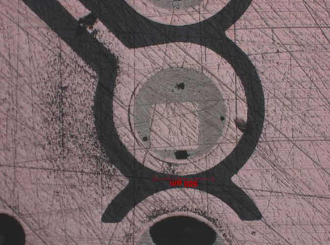
Failure Analysis of a defective printed circuit board
The IEEC was able to determine the cause of a failed impedance testing of a complex Printed Wiring Board (PWB). The team used the design data to isolate the location of termination of the net in question, this was followed by probing PTH connections along the trace and determined where the fail occurred.
Flat sectioning was performed and the image provided was the result. The inner ring around the square feature is the copper plating of the PTH. The appearance of the black ring indicates that the fail was due to drill smear.
Drill smear results when a board is drilled and the holes were not cleaned properly before seed and copper plate. The smear prevents the electrical interconnection of the PTH Wall to the capture pad that connects to the wire going to the other termination point.
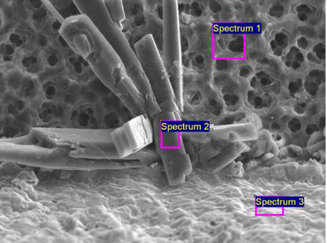
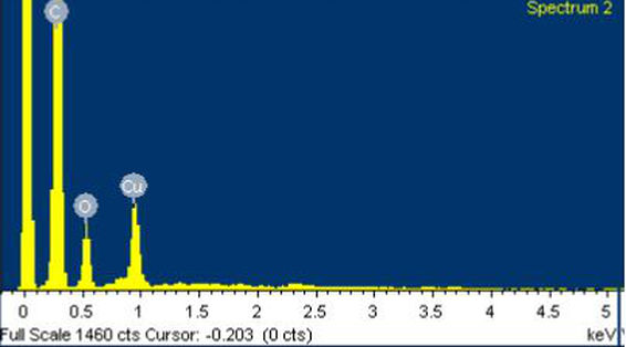
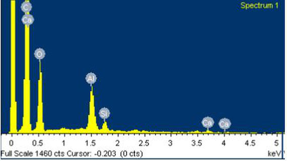
Temperature humidity bias test failure
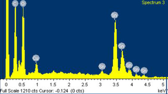
We received a request from one of our partners to attempt to replicate the abnormal test results that they were getting internally. The board had some exposed wires coated with a tin coating.
Wiring up new boards and setting up our Temperature/Humidity chamber, we were able to reproduce their test results after 1100 hours.
The resistance measurements were in the order of 1M. FA of these parts showed that the dendritic growth from the surface of the Copper traces were made up of copper and tin.
SEM imaging with EDX confirmed the constituents of the dendrites as being Copper, Sulfur and possibly CuSO4.