Our 36th Annual Electronics Packaging will be held in-person this year at GE Aerospace Research Campus in Niskayuna NY.
Here are the confirmed speakers for our 2025 Electronics Packaging Symposium. This page will fill up with speakers and session chairs as they are confirmed.
Session Chairs and Speakers
Session 0: Keynote Speakers - (Benson Chan)
Speaker: Amanda K Petford-Long (Argonne National Laboratory)

Bio: Amanda Petford-Long is an Argonne Distinguished Fellow in the Materials Science Division (MSD) at Argonne National Laboratory in Chicago. In addition to her own research program, she serves as Director of MSD and of Argonne’s Microelectronics Institute. She has a D.Phil in Materials Science from the University of Oxford and a B.Sc in Physics from University College, London. She moved to Argonne in 2005 from the University of Oxford where she was a full professor in the Materials Department. Her research focuses on nanomaterials and a particular emphasis is on magnetic and resistive-switching nanostructures with potential applications in information storage technology, and on the use of in-situ TEM. She has published over 370 scientific papers. She is a Fellow of the Royal Academy of Engineering, the Royal Microscopical Society, the American Physical Society, and the Materials Research Society. She is a Professor in the Materials Science and Engineering Department at Northwestern University.
Title: Argonne National Laboratory’s Microelectronics Research
Abstract: Microelectronics research at Argonne is encompassed within the Argonne Microelectronics Institute (AMI). Our focus is on pioneering new materials and energy-efficient designs to enable powerful AI-based computing while reducing reliance on critical minerals, and then translating our basic science to manufacturing practices. We use a co-design approach that integrates materials, devices, architectures, software, and applications to transform how our microelectronics research is conducted, and we make extensive use of our co-located user facilities. I will present a few examples of our research, including those outlined in the following paragraph.
Firstly I will discuss how we are using the Advance Photon Source to image the 3D structure of entire integrated circuits with ~10 nm resolution, enabling us to explore defects that affect behavior, and how we are using ultrafast electron microscopy to understand how electric fields drive reversible switching of atomic order in materials. I will present thermal transport models that we are developing to carry out device-scale write cycle simulations of memristive devices, using our exascale computing capabilities. I will also share some of our approaches to modifying the properties of thin films, for example using electromagnetically-enhanced atomic layer deposition.
Speaker: Mark Schultz (IBM)
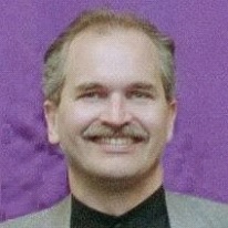
Bio: Dr. Mark Schultz received his B.S. in Engineering from Harvey Mudd College and M.S and PhD in Electrical and Computer Engineering from Carnegie Mellon University. He is currently a Senior Research Scientist at IBM's TJ Watson Research Center. His research interests include data storage systems, computer system packaging, optical packaging, and computer system cooling, with his inventions having been used across a wide range of IBM products including the new IBM Z17 mainframe. He holds 110+ US patents in these and related fields and has authored 40+ published technical papers. He led the experimental portion of IBM’s DARPA ICEcool program and now leads the cold plate portion of IBM’s ARPA-E CoolerCHIPS program and the IBM Research portion of IBM’s System Z thermal solution R&D.
Title: Pumped Two-Phase Cooling for Sustainable High-Performance Computing
Abstract: Recent technology trends in computer systems include movement toward higher compute module power and higher rack power with 3D chip stacks out at the leading edge. These trends result in systems that cannot be cooled with conventional air cooling. Single phase water cooling has been the technology of choice in addressing these trends, but it has risks associated with potential leaks, biological contamination, and freeze damage. It also does not scale down to the very small channels required to cool 3D stacks of large high power chips. An alternative approach is to utilize two-phase flow boiling of a dielectric fluid, which has both benefits and challenges. This talk will present challenges, approaches and results for two phase flow boiling in a near term innovative cold plate implementation as well as in a farther future 3D chip stack embedded cooling configuration. The results demonstrate capability to effectively cool conventional 2D/2.5D systems at a much lower, more sustainable cooling power cost relative to air cooling and the capability to build and effectively cool high power 3D chip stacks while mitigating the risks associated with single phase water.
Session 1: Heterogeneous Integration – Sathya Raghavan & Aakrati Jain (IBM), Gamal Refai-Ahmed (AMD)
Speaker: Manuela Junghähnel (Fraunhofer IZM)

Bio: Manuela Junghähnel has more than 20 years of experience in development of PVD processes,
thin-film technology and new functional materials for large-area and electronic applications
at Fraunhofer Institute for Electron Beam and Plasma Technology FEP, at last as Manager
of the department Sheet-to-Sheet Technologies & Precision Coating. She received 2011
her Doctor of Engineering in the Dept. of Mechanical Engineering in the research field
niobium doped titania as transparent conductive material from Technical University
of Ilmenau, Germany.
Today, Manuela is heading the Center All Silicon System Integration Dresden - ASSID
of Fraunhofer Institute for Reliability and Microintegration IZM, which operates a
state-of-the-art 300 mm process line for 2.5 and 3D wafer level system integration.
Her working field is focused on leading edge advanced packaging and 3D heterogeneous
integration. Beside the activities at IZM-ASSID, Manuela is heading together with
Dr. Wenke Weinreich from IPMS-CNT the Center for Advanced CMOS & Heterointegration
Saxony.
Title: Modular interposer architecture providing scalable heat removal, power delivery, and communication
Abstract: Thermal management based on fluidic cooling is a must for 3D-heterointegration regarding heat dissipation and coolant heat removal capacity. State of the art approaches of fluidic cooling, as back side cold plate cooling or immersion cooling are sufficient for current one tire chip assembly but are not suitable for heat dissipation needs of 3D-stacked high performance chip integration for HPC-applications. New heat removal integration concepts are needed with close distance between coolant and the heat generation. This presentation presents the results of a fluidic micro channels integration in silicon wafer with 50µm remaining silicon distance between coolant and the heat generation circuits. Our silicon integrated heat removal concept enables higher heat removal rates cooling without exceeding of chip junction temperature in the 3D-stack.
Speaker: Chuck Woychik (nHanced Semiconductor)

Bio: Charles Woychik is currently the VP of Sales and Marketing at NHanced Semiconductor, Inc. Previously he was Senior Director of Advanced Packaging Platforms at SkyWater Technology. Chuck has held technical and managerial positions at i3 Microsystems, Invensas, GE Global Research, and IBM. He holds a Doctorate and Masters of Science degree in Materials Science and Engineering from Carnegie-Mellon University. He has a Bachelor’s of Science degree in Materials Science from the University of Wisconsin, Madison. Chuck has numerous publications and 123 issued US patents to his credit.
Title: The Future of Electronics Packaging: Chiplet Architecture and AI Defect Inspection
Abstract: The evolution of chiplet-based architecture is redefining advanced electronics packaging
by enabling heterogeneous integration of multiple high-performance dies within a single
system. As interconnect density and die-to-die bandwidth demands escalate, hybrid
bonding has emerged as a pivotal assembly technology, offering fine-pitch, high-reliability,
low-latency interconnects. Hybrid bonding facilitates direct copper-to-copper (Cu-Cu)
and dielectric-to-dielectric bonding at sub-10µm pitches without the use of solder,
significantly reducing interconnect resistance, capacitance, and thermal bottlenecks
compared to conventional micro-bump and thermocompression bonding methods.
The hybrid bonding assembly process requires stringent surface planarity, ultra-clean
oxide surfaces, precise die alignment, and controlled bonding environments to ensure
defect-free interconnect formation. However, the increasing complexity and scaling
of multi-chiplet packages elevate the risk of bond voids, misalignment, surface contamination,
and oxide dishing — all of which can degrade yield and system reliability. To address
this, AI-driven inspection and defect detection systems are becoming integral to the
hybrid bonding process flow. Using high-resolution optical, infrared, and X-ray imaging
combined with machine learning algorithms, these systems can detect sub-micron voids,
alignment errors, and particle contamination in real-time, providing predictive analytics
to optimize process control and corrective actions.
AI-enabled defect classification systems improve assembly yields by rapidly identifying
root causes of defects and enabling closed-loop feedback for equipment and process
parameter adjustments. Additionally, AI-based predictive maintenance and process drift
detection enhance overall hybrid bonding line uptime and performance. This paper examines
the integration of AI-enhanced defect detection and process control in hybrid bonding
assembly for chiplet-based packaging, discusses the latest advancements in imaging
and data analytics platforms, and outlines future trends toward fully autonomous,
AI-optimized packaging lines supporting next-generation HPC, AI accelerators, and
3D heterogeneous systems.
Speaker: Chris Bower (XDisplay)

Bio: Chris Bower is the Chief Technology Officer and co-founder of X Display Company (XDC). His interests include three-dimensional integration of integrated circuits, heterogeneous integration of compound semiconductors onto non-native substrates and the fabrication of low-cost, large-format electronics using novel assembly methods. Chris is co-author of over 150 publications and co-inventor of greater than 150 US patents.
Title: Heterogeneous Integration of Microscale Light Emitters and CMOS Chiplets Using Elastomer Stamp Mass Transfer
Abstract: Since its inception in the mid-2000s, patterned silicone stamps have been used to perform massively parallel assembly of miniature chiplets onto non-native substrates. In this talk, we will present recent advancements in the elastomer stamp transfer technology and highlight examples of heterogenous systems that were assembled using elastomer stamp mass transfer.
Session 2: Photonics Packaging – John Mazurowski (Penn State Optical Lab), Colin McDonough (AIM)
Speaker: David Harame (AIM Photonics)

Bio: Dr. David Harame is the and the Chief Operating Officer for AIM Photonics and the Associate Vice President of Process Development, Test Assembly & Packaging, and Electronic Photonic Design Automation for the Research Foundation SUNY Polytechnic Institute. David is responsible for the organization’s Photonic technologies, Heterogeneous Integration, Electronic Photonic Design Automation process design kits, and Test, Assembly and Packaging (TAP) operations in Albany and Rochester NY. David Harame is an IEEE Fellow and has held numerous other industry leadership roles throughout his career.
Title: Co-Process and Co-Design for Co-packaged Optics
Abstract: Designing world class Co-Packaged Optic engines requires expertise in photonic integrated circuits (PICs) and electronic-photonic packaging. Systems will typically include custom designed Photonic Integrated Circuits, Dense interconnects to Electronic Integrated Circuits, Interposers/Substrates, Lasers, and Detachable Fiber Array Units (DFAUs). The architecture of the system will determine what components are required. Designing the system requires process design kits for the PICs, Interposer/Substrates, DFAUs. All of these have to be co-designed and the processes need to be matched so there is co-process development required as well as co-package development. Assembly Design Kits are needed to architect the full system with reliabilty and test being important considerations. AIM Photonics has an end-to-end capability of custom PICs and Interposers/Substrates as well as 300 mm wafer and chip scale packaging. This talk will discuss R&D CPO activities of these elements at AIM Photonics.
Speaker: Koushik Ramachandran (Global Foundries)

Bio: Koushik Ramachandran is currently a Principal Technical Staff Member with the Advanced Silicon Packaging Development Group in Globalfoundries, Malta, NY, USA. He’s involved in photonic packaging process and technology development. Prior to joining Globalfoundries, he was an Advisory Engineer in the microelectronics division with IBM, where he worked on 2.5D and 3D packaging development. He received his Ph.D. degree in materials science and engineering from the Georgia Institute of Technology, Atlanta, where he was part of the 3D systems packaging center. He has published his work in various peer-reviewed journals and has presented his work at various materials and packaging conferences.
Title: Photonic Packaging: Path to High Volume Manufacturing
Abstract: Co-packaged optics offer benefits in terms of higher bandwidth density, lower power consumption and enhanced performance. However, optical coupling in photonic packaging remains a significant challenge in terms of scalability for high volume manufacturing. Various optical coupling solutions for realizing scalable, high density photonic packaging will be discussed in this talk. Optical coupling using V-groove fiber attach remains attractive in terms of enabling passive alignment in addition to providing best-in-class fiber-chip coupling performance. Various detachable optical coupling solutions are also being developed to address high fiber count at reduced optical I/O pitch required for AI/ML and data center applications. Some of the detachable fiber coupling solutions will be discussed and compared with passive fiber attach solution. In addition, the integration of light sources on silicon photonics remains a significant challenge. An overview of recent progress made in hybrid integration of laser sources on silicon photonics using a passive alignment method will also be discussed in this presentation.
Speaker: Venkatesh Deenadayalan (RIT)

Bio: Venkatesh is a PhD student in the Microsystems Engineering program at Rochester Institute of technology (RIT), New York, working with Dr. Stefan Preble in the Integrated photonics group. His research is focused on hybrid and heterogenous fabrication and packaging methods for photonic integrated circuits involving photonic wire bonding and micro transfer printing. During his time, Venkatesh has contributed to over 15 published articles and has presented his research at various conferences including Conference in Lasers and Electro Optics (CLEO) and IEEE Electronics Components and Technology Conference (ECTC).
Title: Advanced Photonic Integration and Packaging : Micro‑Transfer Printed Thin Film Lithium Niobate - Silicon Nitride Modulators, and Photonic Wire‑Bonded On‑Chip Lasers
Abstract: In this talk, two distinct manufacturable paths for photonic integration are presented. First, micro transfer printing for enabling the integration of high-performance electro-optic thin films and electrodes onto passive silicon photonic chips to realize high-speed Pockel’s modulators; this discussion covers the coupon fabrication and preparation process, stamp specifications, placement and adhesion control and how these parameters translate into yield and reliability. Second, photonic wire bonding (PWB) using two-photon polymerization is used to couple light from III-V DFB lasers that are die-bonded in a trench of a silicon photonic integrated circuit (PIC) chip. The full assembly process, including die bonding, solder paste dispensing for laser attach is discussed along with the resulting single-mode behavior without mode hops and measured thermal performance.
Session 3: mmWave and 5G Packaging – Jason Case (GE Aerospace)
Speaker: Genaro Soto Valle (Georgia Tech)
Bio:
Title: Zero-Power Additively Manufactured FHE-Enabled Wireless/5G+ Ultrabroadband Modules for IoT, SmartAg, Industry 4.0 and Smart Cities Applications: from dream to reality
Abstract:
Speaker: Michael Holyoak (Bell Labs / Nokia)
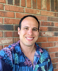
Bio: Michael is a distinguished member of technical staff and the department head of EM Systems & Integration in the RFIC & Packaging Research Lab at Nokia Bell Labs. He leads the development of packaging technologies for RFICs in wireless and sensing networks. His core interests include EM simulation and the design and measurement of passive components including interconnect, filters, and antenna arrays. Prior to joining Nokia Bell Labs, he worked at LGS Innovations, the former U.S. government division of Alcatel-Lucent. Michael is an author and award recipient for his work on mmWave phased arrays and glass-based RFIC packages. He is also an inventor for his contributions made to MEMS tunable filter and multi-band antenna technology.
Title: Radio-on-Glass: A High-Performance Alternative for mmWave Packaging
Abstract: PCB technology is widely used across mmWave application spaces, including 5G wireless communications (24-71 GHz) and automotive radar (24-81 GHz). Advanced processes, such as HDI or ELIC, enable multilayer stack-ups with finer resolution (< 100µm) at a competitive price point for both rigid boards and package substrates. Nokia Bell Labs had pushed PCB processes to their limit in 2018 by creating a fully integrated 384-element phased array at W-band (80-100 GHz) for point-to-multipoint deployment. This array was based on beamformer RFICs assembled into Antenna-in-Package tiles and then onto a common 26-layer PCB. Although the system was successfully trialed, 100 GHz proved to be a distinct barrier for maintaining high-performance in PCB materials and interconnect. Following this milestone, Nokia Bell Labs was tasked to create radios for next-generation wireless backhaul at D-band (141-164 GHz). A new platform for RFIC packaging and RF components that enabled low-loss performance beyond 100 GHz was necessary. This presentation highlights the technological evolution of material, design, and fabrication requirements needed for D-band radio performance and how glass substrates replaced PCB technology for RFIC packages. Various metrology-backed RF components and systems will be presented to demonstrate the strengths of glass substrates and how this new packaging platform provides a solution for Nokia’s future point-to-point wireless links.
Speaker: Sergio Cardona (ED2 Corporation)

Bio: Sergio Cardona is President and CEO of ED2 Corporation, a Tucson-based innovator
in millimeter-wave antennas, 5G/6G radios, and wafer-scale glass products and packaging.
An RF engineer by training, Sergio cut his teeth designing radar and datalinks at
Raytheon, then co-founded two micro-electronics start-ups before acquiring ED2 in
2018 and steering it toward next-generation heterogeneous integration His team has
since unveiled dielectric-waveguide phased arrays, numerous passive components, and
assemblies and sub-assemblies.
Sergio earned a B.S. in Electrical Engineering from Merrimack College and contributes
regularly to Microwave Journal on disruptive mmWave architectures and 3D packaging.
Recognized with Southern Arizona’s Spirit of Philanthropy Award, 2006 Excellence in
Technology Award, 2009 Excellence in Leadership Award, IEEE GOLD founded Boston Chapter,
he also mentors regional STEM programs throughout his career, organically grows engineers
and serves in business and non-profit boards.
On stage, Sergio blends deep technical insight with hard-won manufacturing lessons,
outlining how glass substrates, hybrid bonding, and AI-assisted RF design can tame
the bandwidth, thermal, and cost hurdles facing tomorrows phased-array radars, SATCOM
terminals, datalinks and AI data centers.
Title: From Substrate to System: Unlocking 3DHI for mmWave to Terahertz
Abstract: Bandwidth-hungry phased-array radars, 5G/6G radios, and AI data centers expose a new bottleneck: packaging and interconnect, not transistor speed. As heterogeneous systems merge sensor arrays, RF front-ends, photonics, and high-speed logic into shrinking footprints, organic laminates and even silicon interposers buckle under CTE mismatch, warpage, and dielectric loss. Data rates have jumped 50× and on-chip power density 5×, while spectrum allocations push well into mmWave. ED2’s Advanced Glass Packaging Technology (AGPT™) replaces legacy substrates with wafer-scale fused-silica glass possessing ultra-low dielectric loss, three-times higher thermal conductivity than organics, and a near-perfect CTE match to both silicon and III-V die. AGPT™ enables high-density fan-out routing, laser-drilled through-glass vias, and direct copper-to-copper hybrid bonds, yielding compact 3D system-in-packages that co-integrate RF, photonics, digital logic, and MEMS with essentially zero interconnect penalty. Demonstrated modules include 15–110 GHz T/R tiles 25 % lighter for airborne radar, SATCOM beam-steering arrays surviving −55 °C to +125 °C, 5G/6G radio units with 40 % lower BOM counts, and data-center GPUs whose on-package optical I/O breaks the SERDES power wall. Embedded high-Q glass resonators cut switched-filter-bank insertion loss by 20 % and shrink footprint 30 %, while fluidic microchannels etched into the substrate route coolant under hot spots. Multiple Tier-1 foundries and OSATs have qualified the flow on 200 mm and 300 mm lines, passing 1,000-hour HTOL. ED2 seeks partners to accelerate adoption across defense, telecom, automotive, and cloud sectors.
Session 4: Flexible, Wearable and Additive Electronics – Felippe Pavinatto (GE Aerospace). Mark Poliks (Binghamton)
Speaker: Denis Cormier (Rochester Institute of Technology, AMPrint Center)
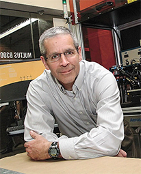
Bio: Denis Cormier is the Earl W. Brinkman Professor of Industrial and Systems Engineering at Rochester Institute of Technology (RIT) where he also directs the New York State funded AMPrint Center. He has 30 years of additive manufacturing experience that includes functional printed electronics processes such as aerosol jet printing, microextrusion, and inkjet printing. Denis is a Fellow of IISE, and he was the 2024 recipient of the International FAME award, which recognizes lifetime achievements related to additive manufacturing R&D.
Title: Additive Printed Electronics Using Molten Metal Droplet Jetting
Abstract: This talk will present an emerging additive printed technology that operates on the principle of on-demand molten metal jetting (MMJ). Rather than using conductive nanoparticle inks, this process melts copper or silver and then jets discrete droplets of the molten metal towards a moving substrate. The droplets cool down and solidify to produce the desired circuit geometry. The resulting printed traces are functionally equivalent to solid core wire with conductivity values matching those of the bulk metal. This is particularly advantageous for high current applications.
Speaker: Christine Kallmayer (Fraunhofer IZM)

Bio: Christine Kallmayer received a diploma in experimental physics in 1994. Afterwards she worked as a research scientist at the research center for microperipheric technologies at the Technical University of Berlin. Her main field of activity was the development and investigation of interconnections using Au-Sn metallurgy. Since 1998 she is responsible for the group “System on Flex” at Fraunhofer IZM. The group is focused on flexible, stretchable and textile electronics. One of the main working areas is the development of new interconnection technologies. The group is also developing new flexible, stretchable and conformable substrate materials, e.g. based on thermoplastic polymers.
Title: Stretchable Electronics - Smart Patches for Wound Monitoring
Abstract: Chronic wounds, which often result from underlying conditions such as diabetes, represent
a major global health burden. Not only are these wounds painful, they are also costly
to treat, often requiring long-term care and regular clinical intervention. A significant
challenge in managing chronic wounds is the difficulty of continuously monitoring
the healing process. Traditional periodic wound assessments are unable to provide
this. This approach is limited as wounds can deteriorate rapidly and subtle changes
may go unnoticed.
In recent years, smart patches have emerged as promising tools to address these challenges.
These wearable devices have embedded sensors that can continuously track wound parameters
in real time. One of the main benefits of smart patches is their ability to monitor
key physiological indicators of wound healing, such as temperature, pH levels and
impedance.
These systems are modular, comprising disposable patches and reusable electronics.
This presentation will describe various smart patch examples. The base technology
involves thermoplastic polyurethane (TPU) substrate with meander-shaped copper (Cu)
tracks. More sustainable base materials are being investigated as promising future
alternatives (e.g. paper), together with printed conductors.
Since the disposable part is in contact with the wound, its surfaces and components
must be biocompatible and must not put pressure on the tissue. As all the complex
and expensive components are intended for the reusable module, the disposable part
is limited to simple electrodes and sensors (e.g. printed pH sensors). Electrode arrays
for impedance spectroscopy have therefore been developed and investigated for suitability
in monitoring wound size.
Speaker: Michael A Cullinan (UT Austin)

Bio: Dr. Cullinan is the director of the Semiconductor Science and Engineering program as well as an Associate Professor in the Walker Department of Mechanical Engineering the University of Texas at Austin. Dr. Cullinan’s research focuses on the development of novel nanomanufacturing systems and on finding ways to exploit nanoscale physical phenomena in order to improve existing macroscale devices and to create novel micro- and nanoscale devices for energy and sensing applications. His research interests include the design and development of nanomanufacturing processes and equipment, metrology of micro and nanomanufacturing, the application of nanoscale science in engineering, the engineering of thin films, nanotubes and nanowires, the manufacturing and assembly of nanostructured materials, and the design of micro/nanoscale machine elements for mechanical sensors and energy systems. Dr. Cullinan has received many awards for his research and teaching including the Outstanding Young Manufacturing Engineer Award from the Society of Manufacturing Engineers (2016), the Rising Star Award from the Sensors Expo and conference (2017), American Society for Precision Engineering Early Career Award (2021), ASME Kornel F. Ehmann Manufacturing Medal (2020), multiple Best Poster Awards from the American Society for Precision Engineering (2017, 2018), and the Outstanding Teaching by an Assistant Professor Award from the Department of Mechanical Engineering at the University of Texas at Austin (2017). Dr. Cullinan is also an associate editor for both Precision Engineering and the ASME Journal of Micro and Nanomanufacturing. In addition, he is the chair of the Micro and Nanotechnology Technical Leadership Committee for the American Society for Precision Engineering. Overall, Dr. Cullinan has published over 150 peer-reviewed journal papers, conference proceedings, book chapters, patents, and technical reports.
Title: Micro and Nanoscale Additive Manufacturing for Electronics Packaging Applications
Abstract: The Nanoscale Design and Manufacturing Laboratory (NDML) at the University of Texas at Austin focuses on the design and development of novel processes and equipment for the manufacturing of micro and nanoscale devices and structures. This talk will focus on two new microscale additive manufacturing processes, known as Holographic Metasurface Nano Lithography (HMNL) and Microscale Selective Laser Sintering (μ-SLS), that has been developed in the NDML for the fabrication of 3D electronic interconnect structures. In the HMNL process, sub-wavelength-patterned metasurface masks (metamasks) are used to create multi-colored holograms in a photocurable metal-polymer hybrid resin. This process allows entire 3D, multi-material (insulators and conductors) nanostructures to be patterned using a single light exposure. Preliminary volumetric patterning using this method shows a build rate of over 20 mm3/s in both metals and polymers with sub-micron resolution making it ideal for fabricating redistribution layers for chip packaging applications. In the μ-SLS process, a thin layer of nanoparticle ink is first spread onto the substrate. The substrate is then positioned under an optical subsystem using a custom-built nanopositioning device. A laser that has been focused off a micromirror array is then used to sinter the nanoparticles together in a desired pattern with micrometer resolution. Another layer is then coated onto the substrate and the process is repeated to build up the 3D structure. Finally, the unsintered nanoparticles are washed away to reveal the final 3D part which is well suited for making microelectronic bump structures. This talk will present the materials science, mechatronic systems, optics designs, and process modeling used in both processes to make these additive manufacturing process capable of achieving micrometer resolution with high throughput over large areas (~ 50 mm x 50 mm) and thus break the conventional tradeoff between resolution and throughput in microscale metal 3D printing.
Session 5: Power Electronics / Harsh Environments – David Shaddock (GE), Xaioling Li (NREL)
Speaker: Alan Mantooth (U Arkansas)

Bio: H. Alan Mantooth received the B.S.E.E. and M.S.E.E. degrees from the University of Arkansas, and the Ph.D. degree from Georgia Tech. He spent 8 years at Analogy, a startup company in Oregon. He then joined the faculty of the Department of Electrical Engineering at the University of Arkansas, Fayetteville, where he currently holds the rank of Distinguished Professor. He also holds the 21st Century Research Leadership Endowed Chair in Engineering. His research interests now include analog and mixed-signal IC design & CAD, semiconductor device modeling, power electronics, power electronic packaging, and cybersecurity. Dr. Mantooth is the Executive Director of the UA Power Group and has helped to establish several federally-funded centers of excellence at the UA. He is a Past-President of the IEEE Power Electronics Society (PELS) and currently serves as Editor-in-Chief of the IEEE Open Journal of Power Electronics and Division II Director on the IEEE Board of Directors. Dr. Mantooth is a Fellow of IEEE, a member of Tau Beta Pi, Sigma Xi, and Eta Kappa Nu, and registered professional engineer in Arkansas.
Title: Medium-Voltage Power Module in Data Center Applications
Abstract: This talk will describe the achievement of several power modules that UA has realized at medium voltage levels that provide a basis for data center applications. Some of these modules are examples of heterogeneous developments. Among the key elements to be described are the design tools that effectively enable the power electronics designer to visualize, analyze, and optimize the concepts to be considered. Use of generative algorithms to synthesize possible solutions is an emerging technology. Another key element is effective prototyping capability that enables hardware validation of design concepts. An oft-overlooked component is the design of the derisking test coupons that necessarily layers the design flow where successes stand on other more foundational manufacturing successes. Several case studies are presented up to 10 kV in voltage rating.
Speaker: Jong Eun Ryu (North Carolina State University)

Bio: Dr. Jong Eun Ryu is an Associate Professor of Mechanical and Aerospace Engineering
at North Carolina State University, where he leads the Multiphysics Multiscale Intelligent
Design (MIND) research group. His research focuses on AI/ML-driven co-design for 3D
heterogeneous integration, advanced electronic packaging materials, and multifunctional
nanocomposites. He also serves as Associate Director of Packaging Research at the
Electronic Energy Systems Lab.
Dr. Ryu received his Ph.D. in Mechanical Engineering from UCLA, following his B.S.
and M.S. from KAIST. He previously contributed to semiconductor and nanolithography
technologies as a postdoctoral researcher at UCLA and a Senior R&D Engineer at Intel
Corporation.
His research has been supported by the National Science Foundation (NSF), Air Force
Office of Scientific Research (AFOSR), DARPA, NIH, and other U.S. agencies. He is
an active member of the professional community, serving in leadership roles with ASME
and IEEE. He recently served on the organizing and technical committees for the IEEE
3D Power Electronics Integration and Manufacturing (3D-PEIM) Symposium and is a member
of the IEEE EPS Packaging & Electronics Technical Committee.
Title: Digital Twin for Reliability and Life Prediction in SiC Power Electronics
Abstract: Silicon Carbide (SiC) power electronics are increasingly adopted in applications
demanding high efficiency and thermal stability, such as renewable energy systems,
electric vehicles, and aerospace systems. However, ensuring their long-term reliability
under harsh operating conditions remains a significant challenge. This presentation
introduces a Digital Twin (DT) framework that integrates physics-based modeling with
artificial intelligence (AI) to accurately predict the Remaining Useful Life (RUL)
of SiC power modules and optimize their performance over time.
The proposed framework begins with the development of fracture mechanics-based fatigue
models for critical components such as bond wires and solder layers. These models
are validated through finite element analysis (FEA) and pseudo power cycling tests
(PCT), establishing a reliable foundation for understanding physical degradation.
The framework then extends to a full package-level multi-physics simulation, correlating
electrical failure indicators with mechanical damage. Trained artificial neural networks
(ANNs) enable real-time inference of component health and packaging conditions.
A key innovation lies in using AI to optimize operation parameters—such as output
power and switching frequency—toward a user-defined reliability target. The DT can
predict degradation trends, RUL, and optimal usage scenarios in real time, supporting
predictive maintenance and system-level optimization.
This approach offers significantly higher accuracy than conventional statistical methods,
enabling proactive decision-making for critical infrastructure. It has the potential
to improve energy efficiency, reduce maintenance costs, and enhance safety in mission-critical
applications.
Speaker: Fang Lou (Stonybrook University)
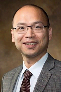
Bio: Dr. Fang Luo (S’06- M’10- SM’13) is SUNY Empire Innovation Associate Professor in the ECE Department and Spellman High Voltage Power Electronics Lab director at Stony Brook University, Stony Brook, New York. His research interests include advanced grid-tied converters, HVDC systems and its economic-technical modeling, high-voltage/high power-density converter design, EMI, and advanced power module packaging/integration for wide band-gap devices. Dr. Luo is a senior member of IEEE. He holds three US patents and has authored/co-authored more than 50 journal papers and 150 peer-reviewed conference papers, and one book. He is an Associate Editor of IEEE Transactions on Power Electronics. He is a recipient of the NSF CAREER Award. He was an Assistant Professor in the Electrical Engineering Department at the University of Arkansas (17’-20’) and a research assistant professor at the Ohio State University (14’-17’).
Title: Advanced Packaging and Optimization for High Voltage WBG Modules
Abstract: This presentation will cover the latest research from the author’s group on high-power, high-voltage SiC module packages and GaN module packages using double-sided cooled structures. The speaker will discuss challenges in these module designs, such as interconnection issues, EMI mitigation, and fabrication processes, and propose potential solutions. The presentation will cover the presenter’s work on the Design-of-Reliability and Power Module Packaging Assembly Kit development.
Session 6: Future of Computing for HPC / AI
Speaker: Clint Schow (UC Santa Barbara)

Bio: Clint Schow received B.S., M.S. and Ph.D. degrees from the University of Texas at Austin. After positions at IBM and Agility Communications, Dr. Schow spent more than a decade at the IBM T.J. Watson Research Center in Yorktown Heights, NY, as a research staff member and manager. Since 2015 he has been a professor in the Electrical and Computer Engineering Department at the University of California Santa Barbara. He is a fellow of the IEEE and Optica, has published more than 250 journal and conference articles, and has 33 issued patents.
Title: Low-Power Coherent Optics to Enable Reconfigurable Networks in AI Systems
Abstract: Energy-efficient coherent links offer a path to minimizing power consumption and latency while enabling bandwidth scaling and expanded optical link budgets that can enable reconfigurable photonic networks tailored to the demands of AI workloads.
Speaker: Vikas Gupta (Global Foundries)

Bio: Vikas Gupta is the Senior Director of Product Management at GlobalFoundries focused on Silicon Photonics and ancillary technologies. Prior to the current role, he was the Vice President of Design Systems at POET Technologies. Vikas has a MS in Electrical Engineering from the University of Texas and an MBA from the University of Massachusetts at Amherst.
Title: Silicon Photonics Technology and Packaging: An AI Perspective
Abstract: The presentation will explore the transformative potential of silicon photonics in
advancing artificial intelligence (AI). The session will highlight the development
of new architectures that will drive co-packaged optics (CPO) and support higher fiber
counts, comparing scale-up within single racks and across multiple racks. It will
delve into SiPh architectures, contrasting pluggable modules with scale-up CPO, and
will introduce the GF Fotonix™ platform—a comprehensive foundry solution that will
feature advanced components such as micro-ring modulators, high-bandwidth Ge photodiodes,
and high-power SiN primitives.
The presentation will cover innovative fiber coupling technologies, including the
250 µm-pitch V-groove Si Fiber Coupler and the 127 µm-pitch V-groove SiN Fiber Coupler,
emphasizing their scalability and performance. Additionally, it will discuss the building
blocks for detachable fiber couplers, which will enhance alignment tolerance and integration
into the GF Fotonix™ platform.
The session will conclude with an overview of test methods for optical interconnects
and the critical role that packaging and testing will play in the adoption and scaling
of CPO. This presentation will underscore the significant advancements in silicon
photonics and their implications for the future of AI.
Speaker: John Knickerbocker (IBM)

Bio: Dr. John U. Knickerbocker received his PhD degree in 1982 from the University of Illinois studying materials science & engineering. Dr. Knickerbocker is an IBM Distinguished Engineer and member of IBM Academy. He leads research programs in the Chiplet & Advanced Packaging Team at IBM and has over 40 years of experience between IBM Microelectronics and IBM Research. Dr. Knickerbocker has authored or co-authored over 400 patents / patent applications and more than 100 technical papers, presentations, and publications. He has over 18+ years of participation with the Packaging Technology Committee & ECTC.
Title: Advancements in Co-Packaged Optics from Research to Prototypes & Manufacturing
Abstract: Advancements in co-packaged optics (CPO) technology for artificial intelligence (AI) system adoption benefit from higher bandwidth, low insertion loss, compatibility with lead free solder assembly and compatibility with reliability stress testing. Demonstrated optical link module hardware and continuing hardware advancements permit bandwidth density scaling from 4 to 8 optical links per millimeter on photonic integrated circuit (PIC) chips to 20 to 50 optical links per millimeter of chip edge. Compatibility with wavelength division multiplexing support multiple lambda per optical channel to compliment physical density scaling. In addition, optical channel scaling per module while maintaining compatibility with pluggable connector industry standards permit overall on and off module photonic chip to chip scaling by orders of magnitude. CPO technology advancements from research laboratory to prototyping and manufacturing leverage co-design, modeling and simulations through iterative hardware build, integration and characterization. Design, materials, structures and process improvements were made leveraging hardware characterization and updated digital models to match hardware data. A roadmap of next generation of research advancements capture client application form factors with current research product design kits (PDK) / assembly design kits (ADK) and position for next generations of more energy efficient, higher density CPO solutions. Our expanding ecosystem of suppliers, clients and partners using IBM CPO prototyping and manufacturing advancements target continued system adoption and growth for differentiation in targeted AI system applications.
Session 7: Substrates, Platform for Advanced Packaging – Shelby Nelson (Mosaic), Sean Garner (Corning)
Speaker: Erik Jung (Fraunhofer IZM)

Bio: With a background in “physics”, “physical chemistry” and “physics in medicine” from
the University of Kaiserslautern, he joined Fraunhofer IZM in 1994. Heading the group
Advanced Microsystem Assembly, he developed processes in flip chip and chip embedding
technologies eventually expanding his research field into the MEMS/NEMS packaging
and initiated IZM´s MEMS research program in 2005.
Staying from 2007 to 2008 as a research delegate at the University of Utah he was
involved in the packaging of a wireless brain computer interface, establishing the
focus group on Medical Microsystems upon his return to the Fraunhofer IZM. He was
appointed as head of the business sector on medical technologies in 2009.
Since 2015, he is part of IZM´s Business Development Team with a core expertise on
Medical Microsystems. Since 2019, he also serves as liaison manager to Fraunhofer
USA.
Erik is participating as a standing member in conference and roadmap activities of
IEEE-EPS (US) and DGBMT (DE) with his expertise in advanced heterointegration.
In the industrial user interest group IVAM (DE) he has been founding member of the
Wearable Electronics initiative (2014) and is acting board member in the association
for Organic Electronic Saxony (OES) since 2018.
As a part of the Heterogenous Integration Roadmap Task Force of IEEE-EPS, he is co-chairing
the TWG on the System-in-Package activities since 2019.
His professional activities span more than 100 publications, contributions to three
books and numerous invited talks in Germany, France, Norway, US and Asia. He is inventor
or co-inventor in 25 patents.
Title: Evolution of advanced substrate technology: The shifts towards glass as core material
Abstract: High performance computing (HPC) and artificialintelligence (AI) systems are rapidly
pushing legacy package size and I/O limits. Conventional organic substrates suffer
from warpage, thermal and signalintegrity limits, and lack the planarity required
for finepitch interconnects. New glasscore substrates promise to address these limits.
They offer low coefficient of thermal expansion (CTE), uniform expansion, low electrical
loss and excellent planarity, enabling highdensity routing and highaspectratio throughglass
vias (TGVs). Glass core based substrates promise also to hold more chips and allow
for larger packages, making them ideally suited to bridge the gap between organic
carriers and silicon based interposers.
Critical technology challenges to make glass core a reality are TGV drilling and filling,
multi layer high density interconnect routing and large panel handling.
TGV formation relies on advanced processes such as selective laser etching (SLE),
which uses ultrashortpulse laser modification followed by chemical etching.
Also, glass cores enable unique redistributionlayer (RDL) processing. Thinfilm RDLs
fabricated directly on glass provide lowloss fanout of chip and package interconnects
and promise lower cost than silicon interposers while offering similar performance
metrics.
Combined with RDLs, TGVs allow direct electrical connections with small parasitic inductance and capacitance, improved power distribution, and the integration of passive elements on the substrate. Glass core substrates open up further integration perspectives, i.e. for high speed communication and RF systems due to the unique aspects of glass, with its low loss properties and the capability to add optical interconnect directly to the core. Thus, glass core substrates are expected to add to and in some instances replace today´s high density organic substrates and ultra high density silicon interposers , especially bridging the gap between advanced digital technology and the analogue world outside the data center.
The presentation aims to offer insight into recent R&D work on large panel glass core
substrates at Fraunhofer IZM in its role as integration partner for the European APECS
Pilot Line.
Speaker: Robert Schaut (Corning)

Bio: Robert Schaut is a Research Fellow in the Science & Technology division at Corning Incorporated. In this role, he brings materials science expertise to understand interdisciplinary problems and propose novel solutions, including the invention of new glass compositions. He currently leads a team at Corning identifying the mechanical failure modes for glasses used as electronic packaging material and evaluating various solutions to improve its overall reliability.
He earned his B.S. in Ceramic Engineering & Glass Science from Alfred University in
2002 and his Ph.D. in Materials Science and Engineering from The Pennsylvania State
University in 2008. He specializes in the study of chemical and physical properties
of glass surfaces. Since joining Corning in 2008, Robert has conducted research in
glass ceramics, Gorilla® Glasses, and borosilicate and aluminosilicate glasses for
pharmaceutical packaging. He is a co-inventor of Valor® Glass and has co-authored
14 peer-reviewed articles, two book chapters, 140 technical reports, and more than
130 patent applications. Robert has been granted 83 patents and is a member of the
American Ceramic Society.
Title: Addressing mechanical reliability challenges for glass core adoption
Abstract: -
Speaker: Dan Turpuseema (Advantest Interconnect Solutions)

Bio: Dhananjaya (Dan) Turpuseema is Senior Director of Process Engineering at AIS (Advantest Interconnect Solutions), where he leads the development of advanced organic substrate technologies for semiconductor testing and high-performance packaging. With over 32 years of experience in PCB manufacturing, Dan has spent the past six years pioneering processes to fabricate low-volume, high-complexity organic substrates tailored for next-generation applications.
His team’s innovations support fine-pitch designs down to 45 μm, 14-n-14 RDL structures, high pin-count architectures exceeding 90,000 I/Os, and ultra-fine 5 μm line/space geometries—enabling reliable wafer-level probing and multi-die advanced packaging with tight impedance control for high-speed applications.
Dan holds several patents in manufacturing processes and has played a key role in bridging traditional PCB technology with substrate-level precision manufacturing. He holds a Master’s degree in Mechanical Engineering.
Title: Organic Substrate Fabrication for Fine Pitch Wafer Probing and Advanced Packaging
Abstract: The rapid evolution of semiconductor packaging—driven by multi-die architectures, increased I/O density, and high-speed signal requirements—has outpaced traditional substrate manufacturing capabilities. This presentation discusses recent process innovations in the development and production of advanced organic substrates specifically designed for high parallelism wafer-level test and high-performance semiconductor packaging.
Over the past six years, AIS (Advantest Interconnect Solutions) has engineered scalable processes to fabricate low-volume, highly complex organic substrates featuring fine-pitch (≤45 µm), high RDL counts (up to 14-n-14), and fine line/space geometries (5 µm L/S). These substrates support over 90,000 pin counts and meet the stringent impedance, co-planarity control demands of modern high-speed test environments.
We will present key process challenges—including material selection, via reliability, and pattern fidelity—and highlight solutions such as modified semi-additive processes, advanced dielectric systems, and embedded design features for signal integrity and power integrity.
The talk also covers the transition from traditional PCB process flows to precision substrate manufacturing, emphasizing flexibility for low-volume, fast-turn prototyping environments. These innovations are not only critical for enabling effective semiconductor test strategies but are also laying the foundation for next-generation heterogeneous integration.
Attendees will gain insight into the practical manufacturing considerations and technical enablers that are shaping the future of organic substrates for semiconductor test and advanced packaging.
Session 8: Thermal Challenges - Ramchandra Kotecha (GE Aerospace) / Srikanth Rangarajan (Binghamton)
Speaker: Srikanth Rangarajan (Binghamton University)

Bio: Srikanth Rangarajan joined the School of System Science and Industrial Engineering in Fall 2024. He received his M.S & Ph. D in Mechanical Engineering from the Indian Institute of Technology Madras 2017. He obtained his Bachelor in Engineering in 2011 from Anna University Chennai. His research interests include Energy Storage management systems, electronic packaging, Digital twinning for electronics and batteries, Thermal energy storage, Thermal Management of electronics, and Data center cooling. Srikanth is also the author of the book “Phase Change Material Heat Sinks: A multi-objective Perspective.”
Prior to joining the School of System Science and Industrial Engineering, Srikanth worked as an Associate Research Professor in the Department of Mechanical Engineering at SUNY Binghamton.
Title: AI for Energy Efficient Electronic Systems
Abstract: The rise in chip power density has necessitated the development of advanced cooling technologies capable of dissipating significant amounts of heat while maintaining safe operating temperatures. Among these, on-chip two-phase cooling has emerged as a promising and energy-efficient solution. However, the widespread adoption of such technologies is hindered by concerns over reliability, primarily due to a lack of robust models for accurately predicting system performance. A particular challenge is that the failure threshold—known as the critical heat flux—lies close to the desired maximum operating heat flux, making precise prediction essential, ideally with minimal invasive measurements.
Artificial intelligence (AI) is revolutionizing the field of two-phase heat transfer. Recent advancements in AI and machine learning have opened up new possibilities for extracting physically meaningful features previously overlooked, sharing these insights across disciplines, and solving for key physical quantities in phase-change thermofluidic systems based on fundamental principles. In my talk, I will focus on how AI can be leveraged to predict transitions in boiling regimes, highlighting its potential for predictive modeling in two-phase cooling applications.
Speaker: Theodorian Borca-Tasciuc (RPI)

Bio: Dr. Theodorian (Theo) Borca-Tasciuc has a B.S. in Physics from Bucharest University and a Ph.D. in Mechanical Engineering from UCLA. He started his academic career in 2001 at Rensselaer Polytechnic Institute and since 2013 he is a full professor. He is the director of the Nanoscale Thermophysics and Energy Conversion Laboratory (NanoTEC) on the Rensselaer campus. His research interests include fundamental and multiscale investigations of thermal transport and energy conversion particularly in solid-state and development of innovative materials, devices, and systems. He received the NSF CAREER award, School of Engineering Outstanding Team award, is a member of the ASME’s K8 committee on Fundamentals of Heat Transfer, and a member of the ASME's K-9 committee on Nanoscale Thermal Transport. He organized and chaired multiple symposia and sessions on nanoscale thermal transport and energy conversion with ASME, MRS, and CIMTEC International Conferences. Dr. T. Borca-Tasciuc graduated (as main advisor or co-advisor) 20 PhD students and several dozens of Master students. He authored >100 journal articles, several patents and book chapters, has >9600 citations, and h-index of 47.
Title: Thermal conductivity metrology of thin films for electronic applications
Abstract: In chip stacks thermal conduction occurs through the Back End Of the Line (BEOL) layers and bonding layers between multiple chips. To accurately predict temperature profiles and design appropriate cooling solutions, thermal design of next generation chip stacks needs accurate thermal properties for all the layers and interfaces between them. Current state of the art (SoA) for measuring thermal resistance for 3D chip stacks employs test vehicles (TV) with customized microfabricated heaters and thermistors located within the stack. Moreover, SoA determines the thermal resistance only in the direction of layer thickness. However, film stacks are anisotropic and their effective thermal conductivity changes with location.
At Rensselaer Polytechnic Institute (RPI) in the Nanoscale Thermophysics and Energy Conversion lab we developed and employed several techniques for thin film and interface thermal resistance characterization. For effective thermal conductivity measurements of individual and multilayer films on substrate we successfully employed 3ω based techniques, which can determine both in-plane and cross-plane effective thermal conductivity of layers when micro-heaters with dissimilar widths are used. Furthermore, at RPI we developed and employed a non-contact heated-probe Scanning Thermal Microscopy measurement technique that can accurately measure film thermal conductivity with microscale in-plane spatial resolution and we successfully tested it on samples where either the in-plane thermal transport was dominant (high thermal conductivity films on low thermal conductivity substrate) or cross-plane thermal transport was dominant (low thermal conductivity films on high thermal conductivity substrate). These techniques, relevant results, and current developments will be presented.
Speaker: Emad Andarawis (GE Aerospace)

Bio: Mr. Emad Andarawis has over 25 years of experience at GE. He is currently a Principal Engineer of Microelectronics at the GE Aerospace Research. In this role he leads a portfolio of programs in harsh environment sensing, actuation, and control electronics. Most recently, he has been developing high temperature, high reliability electronics with a primary focus on Aviation engines, hypersonics and space applications. Emad holds 96 issued US patents with several additional applications pending.
Emad has a B.S. and M.S. degree in Computer Engineering and Electrical Engineering from Columbia University.
Title: Robust Multilevel Die Interconnect for 600°C Operation
Abstract: High temperature electronics based on SiC continue to advance in complexity and performance
with functionality demonstrated to >600°C and device densities approaching 10,000
devices per die. As the device counts achievable on a single SiC die continue to
increase so does the complexity of on-chip routing.
Die interconnect scaling has not kept up with the demand imposed by the increased
in routing complexity, which results in increased routing overhead which reduces die
area utilization. Highly efficient and scalable routing is needed to support the continued
advancement in high temperature device densities.
The development and characterization of high-temperature multi-level interconnect
is presented. Performance characterization across the temperature range from 25°C
-600°C and the impact of scaling on interconnect resistance, yield, temperature capability
and electromigration performance results is discussed.
Panel Session: Co-Packaged Optics, Challenges and Adoption - John Mazurowski (Director, (ManTech) Electronics Manufacturing Center)
Abstract:
Needs, issues, and events are motivating industry to make co-packaged optics possible. An immediate need comes with supporting information processing using AI, which is driving the needs for electrical power and information processing efficiency. A common issue has been the expense of transmitting optical signals between platforms- fiber / bulk optics / micro-optics / integrated optics / waveguide. Recent events include the availability of optical functions in electronics foundry processes, quantum and neuromorphic computing, the capacity of graphics processing engines, and interconnections between domains provided by efforts in heterogeneous integration. Considering all of these, the definition of co-packaged optics depends on the domain. It is pleasing that industry participants are up to the challenge of making co-packaged optics their own.
Distinguished panelists:
John Knickerbocker (IBM) Presentation Link
Clint Schow (University of San Diego) Presentation Link
Vikas Gupta (Global Foundries)
David Harame (AIM Photonics) Presentation Link
Workshop / Panel / Guest Speaker Podium: Benson Chan (Binghamton University)
The Thursday afternoon will be given to a series of brief talks from companies / organizations
to present who they are, what they research and how you can be a collaborator. We
will have some exciting talks from:
Girish Wable (SMART USA): What is SMART USA and what is a digital twin, how you can be part of the ecosystem.
Scott Miller (NextFlex): Introdution to NextFlex and the world of flexible and hybrid electronics.
John Mazurowski (Penn State): Introduction to Penn State and their work in MANTEC
Dean Turnbaugh (NTVUSA): Advance Additive Processes
Jobert von Eidsen (MKS/Atotech): Advanced Packaging - Substrate Technology Trends